 zu atomic-layer-deposition.de
Atomic-layer-deposition.de

Scientific and education software. Blog of Dr. Sakharov. leokrut.com
Materials related to scientific and education software. Data analysis and crystal growth modeling. Articles mostly of Dr. Sakharov and discussion comments.

Trion Technology - Trion Technology triontech.com
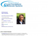
Local Spectroscopy and molecular Systems - P. Lemmens peter-lemmens.de
4Wave, Ion Beam and Biased Target Technology 4Wave Inc. 4waveinc.com
4Wave provides plasma processing equipment, thin film coatings, milling equipment and services to meet vacuum equipment and thin film processing needs.

Home | ASM asm.com
ASM is creating tomorrow’s building blocks, building machines that make it possible to produce even smaller chips. Find out how we’re crafting the future.
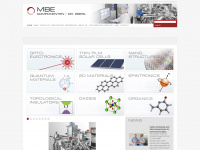
Home - Dr. Eberl MBE-Komponenten GmbH mbe-komponenten.de
Dr. Eberl MBE-Komponenten GmbH develops, manufactures and sells thin film deposition equipment for MBE, surface science and other UHV-applications.
Chipmetrics chipmetrics.com
Neue Domain bei der webgo GmbH feddersen-clausen.de

Homepage - Veeco veeco.com
Veeco designs, manufactures and markets thin film process equipment that enables high-tech electronic device production and development all over the world.
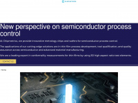
SENTECH: Home of thin film measurement sentech.com
Plasma Etching tools and PECVD & Thin Film Measurement Equipment (Spectroscopic Ellipsometers, Reflectometers) by SENTECH
ALPIN - Atomic Layer Process Innovation Network alpin-germany.de
Atomic Layer Process Innovation Network
NanoQI nanoqi.eu
Multimodal X-ray and Hyperspectral Thin-Film Nano-material Evaluation and Quality Imaging
myplas | advanced coating systems myplas.de
myplas is a product of Plasma Electronic GmbH which includes solutions and equipment for ALD (Atomic Layer Deposition), PECVD (Plasma Enhanced Chemical Vapor Deposition), PEALD (Plasma Enhanced Atomic Layer Deposition) and three dimensional PEALD.
Material Science | News | Materials Engineering | News azom.com
Material Science news, applications, product information, and interviews. Browse the latest Engineering Materials news.

Semiconductor Equipment | CWI Technical Sales | United States cwitechsales.com
CWI Technical Sales is a manufacturers' representative organization offering products and solutions to the Semiconductor, Optoelectronic, Wireless, Defense/Aerospace, Life Sciences and other related industries.

SALD - Spatial ALD Innovators spatialald.com
Spatial Atomic Layer Deposition (Spatial ALD) is a form-following high-quality coating at the atomic level. Compared with conventional ALD, this ingenious technology stacks atomic layers many times faster.
publications Georg Icking-Konert cream-tea.de

ST Instruments | Surface analysis techniques stinstruments.com
ST Instruments carries a complementary range of products with the latest technological innovations, covering every aspect of surface analysis.