 zu wandshop.com
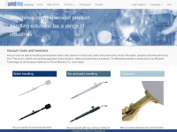
Vacuum handling tools for wafers, die, lense, electronic component semiconductor and parts handling, vacuum pickups/pens.
Windrush Technology. Manufacture machines for the semiconductor industry, wafer handling tools, vacuum wands, tweezers, die handling, lense handling, electronic component handling.
Sprache: Englisch
Samsung Deutschland | Smartphone | TV | Haushaltsgeräte samsung.com
Entdecken Sie die innovative Welt von SAMSUNG Deutschland! Infomieren Sie sich hier über unsere Produkte und finden Sie Hilfe in unserem Support Bereich.
Bildbearbeitungsprogramm | Diashow Programm | Homepage Software | Newsletter Programm in-mediakg.de
Ob Diashow Programm, Bildbearbeitungsprogramm, Newsletter Programm oder Homepage Software - die Programme der IN MEDIA KG sind Made in Germany, intelligent und hilfreich.
Freiberg Instruments - lifetime, single crystal orientation, PID, automation and more freiberginstruments.com
Electrical semiconductor characterization
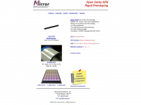
Mirror Semiconductor M-QFN preplated NiPdAu Open Air Cavity QFN Protype IC packaging for MPW Multi-Project wafer MPW foundry shuttle service. Wafer foundries. Pre moulded. Chip Assembly, Chip packages , Open Cavity QFN... . . . . M-QFN8W.65-G5 , M-QFN12W.5-G6 , M-QFN12W.65-G6 , M-QFN12W.8-G6 , M-QFN16W.5-AE , M-QFN16W.5-G6 , M-QFN16W.65-G5 , M-QFN16W.8-G6 , M-QFN20W.4-G6 , M-QFN20W.5-G5 , M-QFN20W.65-G6 , M-QFN20W.8-G6 , M-QFN24W.5-G6 , M-QFN24W.65-G6 , M-QFN24W.8-G6 , M-QFN28W.4-G3 , M-QFN28W.4-G6 , M- mirrorsemi.com
Open Air Cavity QFN Package. Organic Open Cavity for MEMS, RF, Sensors and Semiconductors.
Custom Dicing Hybrid, Semiconductor Wafer Bonding, MEMS wafers customdicing.com
We supply semiconductor wafer, custom dicing hybrid, substrate dicing and all types of dicing at customdicing.com. Get a dicing quotation.
Home - Silicon Wafer Products & Si Wafer Distribution Services - WaferNet, Inc. wafernet.com

Start - Fabmatics fabmatics.com

UnitySC | Leader in Semiconductor Metrology & Inspection unity-sc.com
Explore our metrology & inspection tools for semiconductor yield improvement, specializing in Advanced Packaging, MEM's & unpatterend wafer defect inspection.

X-FAB: X-FAB: Career - Grow your career with the world leading specialty foundry xfabulous.com
We are a team that is passionate about making semiconductor devices that bring value to people's lives, connect people and drive cleaner transportation.

Electronic Minds | Digitalagentur aus Darmstadt, Rhein Main electronic-minds.de
Mit über 2000 erfolgreichen Online-Projekten sind wir Ihr Experte für digitale Kommunikation
ALD Vacuum Technologies - Hightech is our Business ald-vt.com
As the world's leading manufacturer of vacuum equipment for vacuum metallurgy and heat treatment, we employ approx. 900 people in 10 countries. ➤ Read more!
Plume Limited llc plumeltd.com
Home | SPI Supplies 2spi.com
Default Meta Description
Micro to Nano European for all your supplies and consumables for electron microscopy, SEM, FIB, TEM, AFM, light microscopy, sample preparation tools and calibration standards microtonano.com
Micro to Nano is the first truly European company for all your supplies, calibration standards, sample preparation tools and consumables for electron microscopy, SEM, FIB, TEM, AFM and light microscopy. Here you will find practical and innovative products against competitive pricing with a wide range of SEM sample stubs, sample holders, FIB grids, TEM support films and unique calibration tools.